ASML – A Sampling Problem #SWI2007
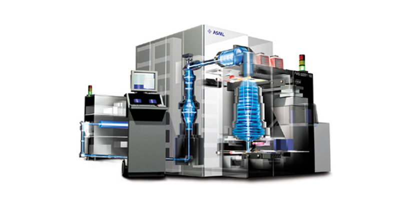
ASML develops machines to perform the very critical lithographic step in the process of integrated circuit manufacturing. Lithography boils down to exposing a photo lacquer (resist) present on a silicon plaque (wafer) with ultraviolet light using a mask (glass plate called reticle with a chrome pattern, derived from the integrated circuit layout, on it). The ASML machine basically is like a commonly known slide projector.
Presently, ASML is working on replacing the reticle with a MEMS (micro-electro-mechanical-system) that consists of millions of tiny tilting mirrors (that together act as a programmable optical grating). In terms of the slide projector above, we are developing a beamer that enables digital CAD data (describing the integrated circuit layout in a vector format) to enter the ASML machine directly, thus circumventing the step of reticle fabrication. Hence, flexibility is increased while the preparation time for our customers is reduced.
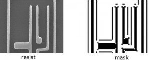
As an example, the figure on the left shows a small part of an integrated circuit imaged in resist on the wafer. The mask clip used to produce this image is shown on the right. Clearly, this clip consists of patterns in the form of polygons that can also be recognized in the resist, and additional polygons that do not print but are used to improve the desired pattern in resist. These additional polygons and vertices are relevant for the problem outlined below as they significantly increase the total number of polygons and vertices.
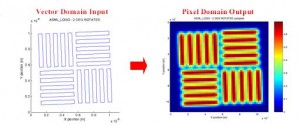
A major technical challenge ASML is facing is the huge amount of large-scale image processing that is needed to convert the conventional mask description into tilt set-points for the millions of mirrors. One of the image processing algorithms is the step in which the vector data describing the mask is transformed into pixel data. This step is known as sampling, which takes a considerable amount of computational operations.
The scale of these computations is roughly the following. The input vector data consists of about 1010 polygons, with in total of about 1011 vertices. These polygons have to be sampled on a grid with a total of 1012 grid pixels, where the polygon edges are not aligned with the grid geometry.
The problem description is the following. Given a list with simple polygons and a sampling grid geometry, calculate the sample (greyscale) value of each grid pixel, such that the residual error in a certain norm is sufficiently small, taking into account that the number of computational operations should be minimal.
Carefully controlling the residual error is important, as for example aliasing errors and discretization errors like stair casing will influence the edge positions of the resulting image. These edge positions need to be controlled with nanometer precision, as they can have a great influence on the electrical performance of the resulting integrated circuit. This for example can affect the maximum clock frequency or the power consumption of the integrated circuit.


